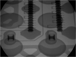
Copper Pillar inside Semiconductor Packaging. The analysis of this Copper Pillar attachment requires 3D CT.
3D CT provides "section image" of the object at any angle, at any view. Above section images of Copper Pillar show pattern open caused by voids.
Defected object can be visualized in 3D rendering image too. Above images show exact location of voids which caused the pattern open.


No comments:
Post a Comment